- Anormal priority encoder encodes only the highest-order data line. But in many situations, not only the highest but the second-highest priority information is also needed.
- The circuit presented here encodes both the highest-priority information as well as the second-highest priority information of an 8-line incoming data.
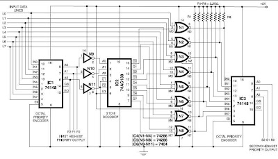
- The circuit uses the standard octal priority encoder 74148 that is an 8-line-to-3-line (4-2-1) binary encoder with active-‘low’ data inputs and outputs.
- The first encoder (IC1) generates the highest-priority value, say, F. The active- ‘low’ output (A0, A1, A2) of IC1 is inverted by gates N9 through N11 and fed to a 3-line-to-8-line decoder (74138) that requires active-‘high’ inputs.
- The decoded outputs are active-‘low’. The decoder identifies the highest-priority data line and that data value is cancelled using XNOR gates (N1 through N8) to retain the second- highest priority value that is generated by the second encoder.
- To understand the logic, let the incoming data lines be denoted as L0 to L7. Lp is the highest-priority line (active-‘low’) and Lq the second-highest priority line (active-‘low’). Thus Lp=0 and Lq=0. All lines above Lp and also between Lp and Lq (denoted as Lj) are at logic 1.
- All lines below Lq logic state are irrelevant, i.e. ‘don’t care’. Here p is the highest-priority value and q the second-highest-priority value. (Obviously, q has to be lower than p, and the minimum possible value for p is taken as ‘1’.) Priority encoder IC1 generates binary output F2, F1, F0, which represents the value of p in active-‘low’ format.
- The complemented F2, F1, and F0 are applied to 3-line-to-8-line (one out of eight outputs is active-‘low’) decoder 74138. Let the output lines of 74138 be denoted as M0 through M7. Now only one line is active-‘low’ among M0 through M7, and that is Mp (where the value of p is explained as above).
- Therefore the logic level of line Mp is ‘0’ and that of all other M lines ‘1’.
- The highest-priority line is cancelled using eight XNOR gates as shown in the figure.
- Let the output lines from XNOR gates be N0 through N7. Consider inputs Lp and Mp of the corresponding XNOR gate. Since Mp = 0 and also Lp = 0, the output of this XNOR gate is Np = complement of Lp = 1.
- All other L’s are not changed because the corresponding M’s are all 1’s. Thus data lines N0 through N7 are same as L0 through L7, except that the highest-priority level in L0 through L7 is cancelled in N0 through N7.
- The highest-priority level in N0 through N7 is the second-highest priority leftover from L0 through L7, i.e. Nq=0 and Nj=1 for q≤7. Now these N lines are applied to priority encoder 2 (IC3) to generate S2, S1, S0, which represent q. Thus the second-highest priority value is extracted.
- Through cascading one can recover the third-highest priority, and so on.
- For example, let L0 through L7 = X X X 0 1 1 0 1.
- Here the highest ‘0’ line is L6 and the next highest is L3 (X denotes ‘don’t care’). Thus p=6 and q=3.
- Now the active-‘low’ output of the first priority encoder will be F2 F1 F0 = 0 0 1. The input to 74138 is 1 1 0 and it outputs M0 through M7 = 1 1 1 1 1 1 0 1. Since M6=0, only L6 is complemented by XNOR gates.
- Thus the outputs of XNORs are N0 through N7 = X X X 0 1 1 1 1. Now N3=0 and the highest priority for ‘N’ is 3. This value is recovered by priority encoder 2 (IC3) as S2 S1 S0 = 1 0 0.
- Using the circuit of direct-conversion receiver described here, one can listen to amateur radio QSO signals in CW as well as in SSB mode in the 40-metre band.
- The circuit makes use of three n-channel FETs (BFW10). The first FET (T1) performs the function of ant./RF amplifier-cum-product detector, while the second and third FETs (T2 and T3) together form a VFO (variable frequency oscillator) whose output is injected into the gate of first FET (T1) through 10pF capacitor C16.
- The VFO is tuned to a frequency which differs from the incoming CW signal frequency by about 1 kHz to produce a beat frequency note in the audio range at the output of transformer X1, which is an audio driver transformer of the type used in transistor radios.
- The audio output from transformer X1 is connected to the input of audio amplifier built around IC1 (TBA820M) via volume control VR1.
- An audio output from the AF amplifier is connected to an 8-ohm, 1-watt speaker.
- The receiver can be powered by a 12-volt power-supply, capable of sourcing around 250mA current.
- Audiooutput stage can be substituted with a readymade L-plate audio output circuit used in transistor amplifiers, if desired.
- The necessary data regarding the coils used in the circuit is given in the circuit diagram itself.

- The circuit of a 7MHz C W / A M QRP transmitter described here can be used to transmit either CW or audio frequency Modulated signal over a 7MHz carrier.
- The carrier frequency oscillator is crystal controlled using 7MHz crystal in its fundamental mode.
- The tank circuit comprises a shortwave oscillator coil which can be tuned to 7MHz frequency with the help of ½J gang capacitor VC1.
- Transistor T2 (with identical tank circuit connected at its collector as in case of transistor T1) serves as a power amplifier.
- The RF output from oscillator stage is inductively coupled to the power amplifier stage.
- The output from power amplifier is routed via capacitor C3 and inductor L3 to a half-wave dipole using a 75-ohm coaxial cable. ½J gang capacitor VC3 along with inductor L3 forms an antenna tuning and matching network between the output of power amplifier stage and coaxial transmission line for maximum power transfer. Suitable heat sink should be used for transistor T2.
- Tuning adjustments may be accomplished using a 6-volt torch bulb. Connect the bulb to the collector of transistor T1 first through a coupling capacitor and tune ½J gang VC1 for maximum brilliance.
- Note: the bulb would light according to intensity of RF energy.
- Same procedure may be repeated for power amplifier stage and antenna tuning network for ensuring maximum power transfer.
- For CW operation, switch S1 is to be kept on for bypassing the audio driver transformer and Morse key is used for on/off-type modulation. CW would be generated during key depressions.
- For AF modulation, Morse key points should be closed and switch S1 should be flipped to ‘off’ position. Any suitable mike. Amplifier may be used to feed audio input to the audio driver transformer X1.
- For transformer X1 you may use the transistor-radio type AF driver transformer.

- This equaliser uses low-cost op-amps.
- Good-quality op amps powered by a single voltage supply are readily available in the market.
- The op-amp should have a noise density of less than 24nV/√Hz, slow rate of more than 5V/μs and gain bandwidth product greater than 3 MHz. The NE5532 or LM833 used in this circuit meets these requirements.
- Equalizer circuits typically divide the audio spectrum into separate frequency bands and have independent gain control for each band. The output of each band is mixed at IC4(A) and then fed to an audio power amplifier.
- Proper quality factor (Q) needs to be selected to avoid overlap in adjacent bands as this introduces coloration into the audio signal.
- We have used the multiple-feedback band pass filter topology shown in left-most corner at the bottom of the figure.

- This is a circuit for single-channel band pass filter. If the capacitors are of the same value, the calculations are fairly simple. For calculating the component values, use the following formulae:
- Centre frequency (fo) : 1/2πC√(Ra||Rb) Rc
- Bandwidth (B) : 1/πCRc
- Quality factor (Q) : fo/B = πfoCRc
- Gain (A) : –Rc/2Ra
- These can be combined to give the following formulae:
- Ra = Q/2πfoAC
- Rb = Q/2πfoC (2Q2–A)
- Rc = Q/πfoC

- Begin the calculations by choosing a large value of capacitance (~0.1F) and smaller value of resistances. Increasing the capacitance decreases resistances (Ra, Rb and Rc).
- Care must be taken to avoid overloading on the input buffer op-amp. Note that stray capacitances on the board reduces the value of ‘C.’ The bandwidth and gain do not depend on Rb. Hence, Rb can be used to modify the mid-frequency without affecting the bandwidth and gain. For equalisers, there are standard mid-frequencies that are normally used.
- The exact frequencies depend on the octave division, application and some degree of manufacturers’ preference, but nearly all share the basic octave boundaries that are based on a centre frequency of 1000 Hz. A balance between the number of filters and bandwidth need to be observed.
- It is possible to use a wider bandwidth and fewer filters, or narrower bandwidth and more filters. Anything narrower than 1/3 octave is rare, since the complexity of the filters increases for higher values of ‘Q.’
- This can get rather expensive and in reality is of limited use for most applications in audio systems. National Semiconductor lists the following mid-frequencies for a 10- band graphic equaliser: 32, 64, 125, 250, 500, 1k, 2k, 4k, 8k and 16k. It also recommends a ‘Q’ of 1.7 for equalisers.
- The table lists the component values for different centre frequencies of the equaliser. We used ‘Q’ of 1.7 and gain (A) of 4.
- The circuit for the 5-band equalizer uses IC1 (A) LM833 as the buffer stage for the equaliser. It is a non-inverting amplifier with a gain of ‘2.’ The input signal is divided by ‘2’ by the resistive network comprising R3 and R4.
- Hence the net gain of this amplifier is unity. Two 100k resistors (R1 and R2) are used as a voltage divider and the junction voltage is fed to its positive input through R6. This divider has enough power to feed all other op-amps directly.Resistor Ro (R8=R12=R16=R20=R24=R28=R30=100Ω) has the dual function of noise reduction and resistive isolation of capacitive load. It may be varied between 50 and 150 ohms depending on the noise in the circuit.
- The potmeters (VR1 through VR5) are in the signal path and hence should be of the best quality possible. Wrap the body of the pots with bare copper wire and solder the other end of the wire to ground. Since the filters are very sensitive, all resistances should be metal-film type and the capacitors should be polyester type.
- Each stage of the op-amp needs to be capacitively coupled to the next stage so that the DC does not get propagated and amplified. For a good low-frequency response, this coupling capacitor should be greater than 1 μF. A 10μF, 16V capacitor is used in each stage of the circuit here.
- The circuit is powered by a 12V DC regulated supply. A well-regulated supply using 7812 is recommended. Ground the Vcc pin of each op-amp with a 0.1μF ceramic disk capacitor to bypass the noise.

- The circuit presented here can be used for connecting two telephones in parallel and also as a 2-line intercom.
- Usually a single telephone is connected to a telephone line. If another telephone is required at some distance, a parallel line is taken for connecting the other telephone.
- In this simple parallel line operation, the main problem is loss of privacy besides interference from the other phone. This problem is obviated in the circuit presented here.
- Under normal condition, two telephones (telephone 1 and 2) can be used as intercom while telephone 3 is connected to the lines from exchange.
- In changeover mode, exchange line is disconnected from telephone 3 and gets connected to telephone 2. For operation in intercom mode, one has to just lift the handset of phone 1 and then press switch S1.
- As a result, buzzer PZ2 sounds. Simultaneously, the side tone is heard in the speaker of handset of phone 1. The person at phone 2 could then lift the handset and start conversation. Similar procedure is to be followed for initiation of the conversation from phone 2 using switch S2.
- In this mode of operation, a 3-pole, 2-way slide switch S3 is to be used as shown in the figure. In the changeover mode of operation, switch S3 is used to changeover the telephone line for use by telephone 2.
- The switch is normally in the intercom mode and telephone 3 is connected to the exchange line. Before changing over the exchange line to telephone 2, the person at telephone 1 may inform the person at telephone 2 (in the intercom mode) that he is going to changeover the line for use by him (the person at telephone 2).
- As soon as changeover switch S3 is flipped to the other position, 12V supply is cut off and telephones 1 and 3 do not get any voltage or ring via the ring-tone-sensing unit. Once switch S3 is flipped over for use of exchange line by the person at telephone 2, and the same (switch S3) is not flipped back to normal position after a telephone call is over, the next telephone call via exchange lines will go to telephone 2 only and the ring-tone sensing circuit will still work.
- This enables the person at phone 3 to know that a call has gone through. If the handset of telephone 3 is lifted, it is found to be dead. To make telephone 3 again active, switch S3 should be changed over to its normal position.


